

Advanced Package Failure Analysis Workshop
Live Seminar & Workshop at UTS- 00 years
- 00 months
- 00 days
- 00 hours
- 00 minutes
- 00 seconds


Joint Workshop Partner
ZEISS would like to thank the Semiconductor Sector Service Bureau for working with us on this workshop.

Overview
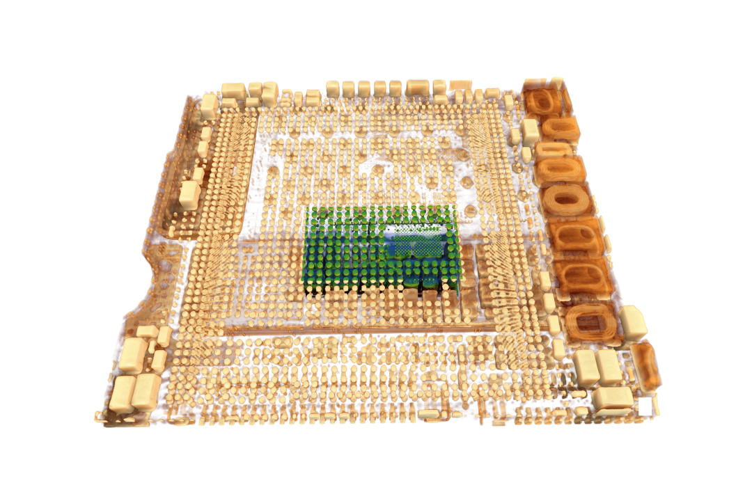
In the post-Moore era, advanced packaging is becoming more critical to meet the booming demands of electronic products with smaller size, more powerful performance and lower cost. As the semiconductor industry continues to evolve, the complexity of devices is on the rise, leading to new challenges in failure analysis. New package architectures introduce more complex defects that are buried deep below many layers, challenging the entire failure analysis workflow – from electrical characterisation to physical analysis and root cause determination. Traditional workflows for high-resolution package analysis of buried features lack the required combination of speed, resolution, and 3D information to understand the problems.
Learn how these advancements help you to identify, access, prepare and analyse regions of interest in advanced package architectures!


Luna Zhang holds a Master of Science in Materials Science and Engineering from National University of Singapore. Luna has 4 years' experience in failure analysis and advanced microscopy techniques, with a strong background in semiconductor technologies. Having previously worked as a Failure Analysis Engineer at Micron Technology, Luna gained extensive hands-on experience in identifying and resolving complex issues in semiconductor packaging. Currently, Luna serves as an APAC X-ray Microscopy Product Application Specialist at ZEISS, where she leverages her expertise to help customers in the Asia-Pacific region optimize their workflows. With a passion for advancing failure analysis solutions, Luna is committed to driving innovation and delivering unparalleled precision in semiconductor diagnostics.
Register for the workshop here
After attending the workshop, you will receive:
- An e-book on Semiconductor Packaging Failure Analysis